Building an 8-bit computer in LSim
In this blog post we’ll take a lot at a (very) simple 8-bit computer I designed in LSim, a digital logic simulator I wrote as a hobby project. The computer itself is inspired by Ben Eater’s YouTube series “Build an 8-bit computer from scratch”.
Overview
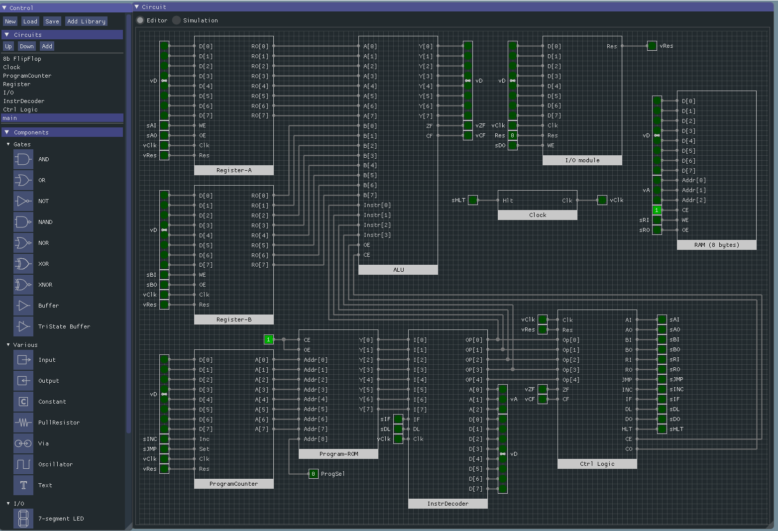
The computer is constructed from several basic building blocks:
- Two 8-bit registers: A and B
- an Arithmetic Logic Unit (ALU)
- a clock-module
- the I/O module provides the interaction with the end-user
- the program counter keeps track of the current position in the program
- the program ROM contains the code to execute
- an instruction decoder to decipher the program ROM
- the Control Logic Unit links opcodes to the signals that control all the modules
- a little bit of random access memory (RAM)
The register module
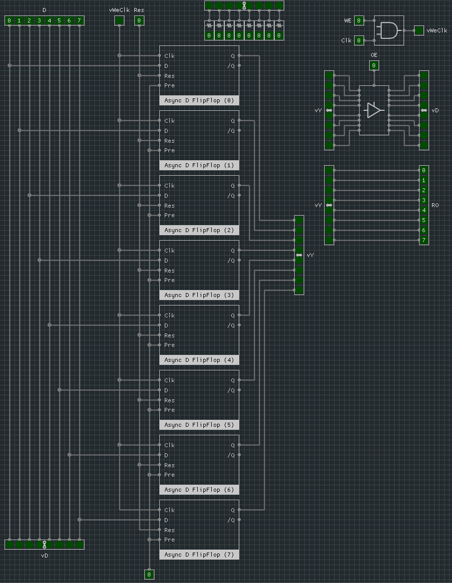
The register-module is connected to the data-bus D[0:7] and stores data on the rising edge of the Clk-signal when WE (write-enable) is asserted. When OE(output-enable) is asserted the data is written back to the data-bus. The register data is always available on the RO-bus which is connected to the ALU. When the RES-signal is asserted the register is reset to all zeros.
Internally the register is constructed using 8 1-bit D-flipflops.
The Arithmetic Logic Unit
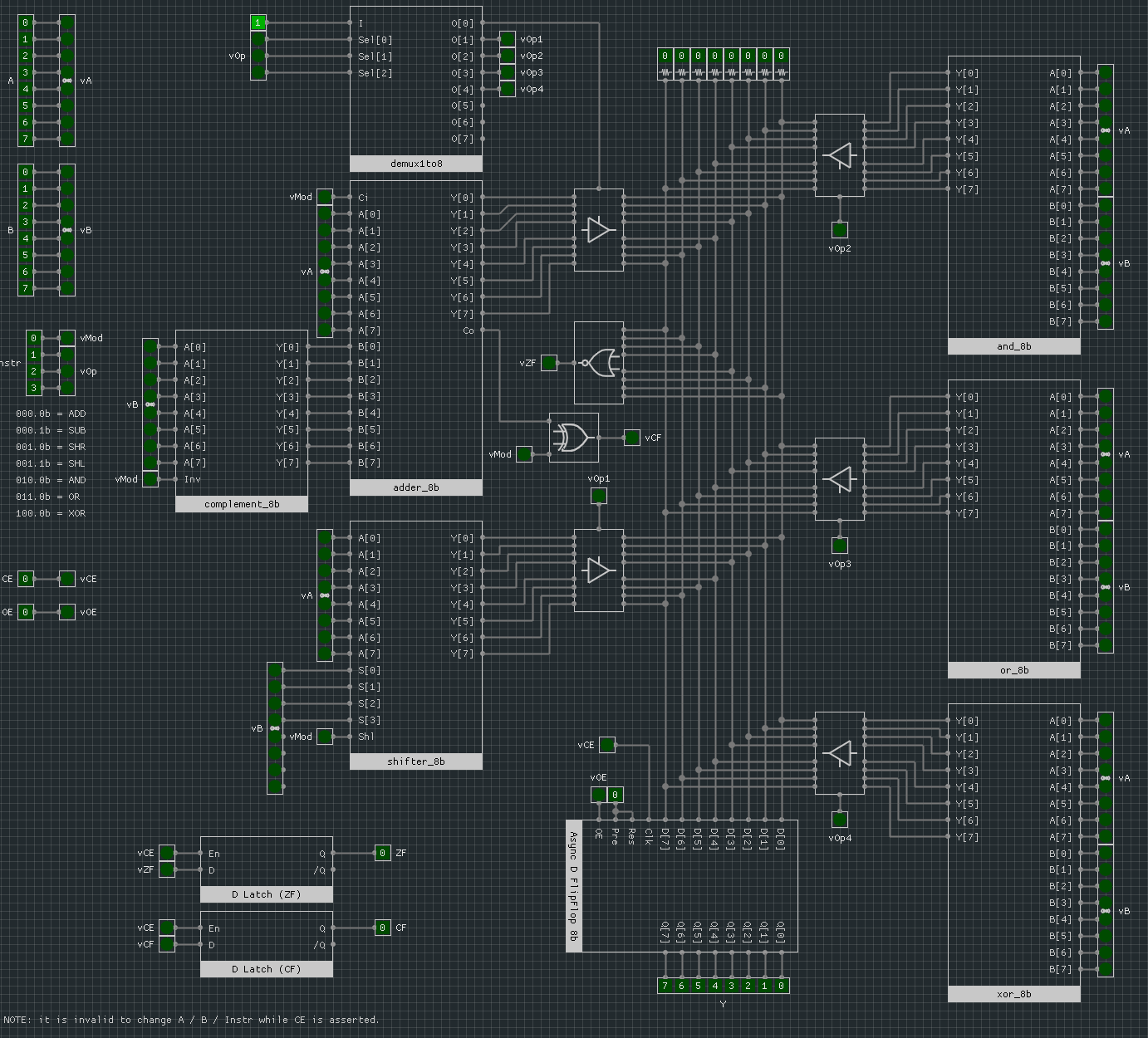
The ALU is the biggest module of the CPU. It takes the values of the two register-modules as inputs and outputs the result to the data-bus D[0:7]. The ALU provides multiple operations. These operations are always computed and the Instr is used to decide which operation will be stored in the output buffer latch when CE (computation enable) is asserted.
The Instrinput is 4-bits wide but only the top 3-bits are used to select the operation sub-module to enable. The low bit can be used as a modification flag to the active unit, i.e. it’s used to switch the adder-module to a subtraction operation. An overview of currently supported operations:
| [3:3] | [2:2] | [1:1] | [0:0] | Operation |
|---|---|---|---|---|
| 0 | 0 | 0 | 0 | Add |
| 0 | 0 | 0 | 1 | Subtract |
| 0 | 0 | 1 | 0 | Shift-Right |
| 0 | 0 | 1 | 1 | Shift-Left |
| 0 | 1 | 0 | 0 | Bitwise AND |
| 0 | 1 | 1 | 0 | Bitwise OR |
| 1 | 0 | 0 | 0 | Bitwise XOR |
As mentioned earlier, the result of the computation is buffer using an 8-bit D-flipflop. This allows the ALU to ‘capture’ the state of the input-registers when CE is asserted. Later, when OE(Output Enable) is asserted the result can be written to the data-bus independent of the current state of the input.
Two extra buffer flags are output by the ALU: ZF(Zero Flag) is asserted when the last computation resulted in a zero and CF(Carry Flag) is asserted when the last operation was an addition or subtraction generated a carry or borrow out of the most significant bit position.
The clock module
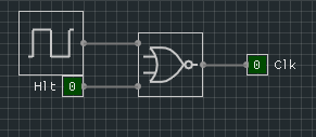
The clock-module is a small module that plays a big role in the computer. All other modules synchronize their operations using the signal generated by this module. When the Hlt-signal is asserted no output is generated and the computer stops running.
The Input-Output module
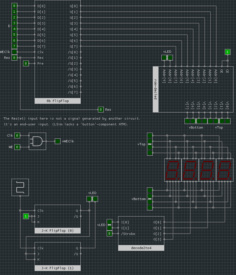
The I/O-module is the place where the user interacts with the computer. It has a display using 7-segment LED modules to show the value of the data-bus.
It would normally also have a reset button but that component has not been implemented in LSim yet. Instead, it’s replaced with a regular input-connector on the main circuit (users can’t interact with connectors in nested circuits).
The value on the data-bus is stored in a local 8bit D-flipflop on the rising edge of the clock when the WE-signal is asserted. The value of that flipflop is fed as part of the address of the decoder ROM. In turn, the output of the decoder ROM is used to light up the required segments of the 7-segment LED module. Each digit is decoded in sequence and displayed for a short time. If this runs at a high enough frequency it’s perceived as a solid display by the user due to the persistence of vision effect.
A brief interlude: ROMs in LSim
When implementing read-only memory in LSim I had a choice. I could add an extra component to LSim which loads data from a binary file and returns the addressed byte (or word). At run-time, this would be the most performant. But it would also mean adding another type of dependency to a circuit, the binary file.
So I chose to go down another path and simulate the entire ROM using components already defined in LSim. I wrote the rom_builder-script that uses the LSim Python-bindings to read a binary file and spit out a LSim circuit that hardcodes the data in the ROM. For larger ROMs it generates a nested set of circuits.
The resulting ROM-circuit can be used in LSim as any other reference circuit library. One shortcoming of the current script is that it doesn’t arrange the components nicely on the circuit diagram.
The binary data for the ROM that’s used as a 7-segment LED decoder in the I/O-module is generated using another small Python-script. This script runs independently from LSim, and its output could also be used to program a real physical ROM-chip.
The Program Counter
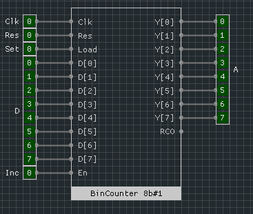
The program counter keeps track of the current position in the executing program. It’s implemented using an 8-bit binary counter that is incremented on the rising edge of the clock when the Inc-signal is asserted.
A value can also be loaded directly in the counter to jump to a specific address. When the Set-signal is asserted, the value currently on the data-bus is stored in the counter. Finally, when the Res-signal is asserted the program counter is reset to zero.
The output of the Program Counter is connected to the address lines of the Program ROM.
The Program ROM
The program-ROM contains the executable code to run. A program is a sequence of 8-bit opcodes. Some opcodes are followed by an 8-bit data element.
The lower 5-bits of an opcode specify the instruction to execute and the upper 3-bits specify an optional memory (RAM) address used by the instruction.
Additionally, instructions are split into two groups as indicated by the top bit of the instruction. Instructions with a one-bit use the ALU and in that case the lower 4-bits specify the ALU-operation to execute. The remaining instructions do not use the ALU.
The currently defined instructions are :
| Mnemonic | Opcode[0:4] | Operation | Data |
|---|---|---|---|
| NOP | 0b00000 (0) | No Operation | No |
| LDA | 0b00001 (1) | Load Register-A from memory | No |
| LDB | 0b00010 (2) | Load Register-B from memory | No |
| LTA | 0b00011 (3) | Load literal into Register-A | Yes |
| LTB | 0b00100 (4) | Load literal into Register-B | Yes |
| STA | 0b00101 (5) | Store from Register-A to memory | No |
| STB | 0b00110 (6) | Store from Register-B to memory | No |
| PRA | 0b00111 (7) | Output Register-A to display | No |
| JMP | 0b01000 (8) | Jump to address | Yes |
| JZ | 0b01001 (9) | Conditional Jump (zero-flag set) to address | Yes |
| JC | 0b01010 (10) | Conditional Jump (carry-flag SET) to address | Yes |
| HLT | 0b01111 (15) | Halt CPU | No |
| ADD | 0b10000 (16) | Add register-B to register-A (result in register-A) | No |
| SUB | 0b10001 (17) | Subtract register-B from register-A (result in register-A) | No |
A simple program that counts through all integer values, wrapping around, looks like:
LTA, 0   # move 0 into register-A
LTB, 1   # move 1 into register-B
PRA      # display register-A
ADD      # add register-B to register-A
JMP, 4   # jump to address 4 (=> PRA instruction)
The instruction decoder
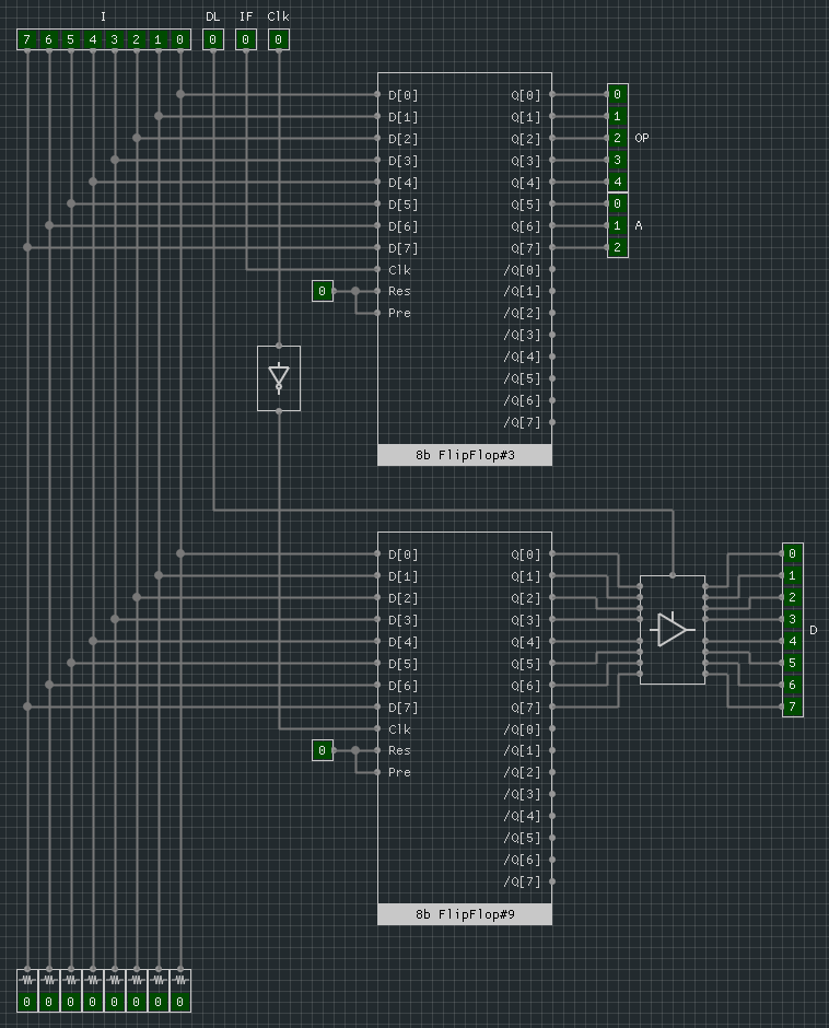
The instruction decoder takes the output from the program-ROM and processes it depending on the state of the input signals. When IF(Instruction Fetch) is asserted the data is latched and split into the instruction and address parts and output on the OP and A pins. when DLis asserted the byte is sent to the data-bus.
The Control module
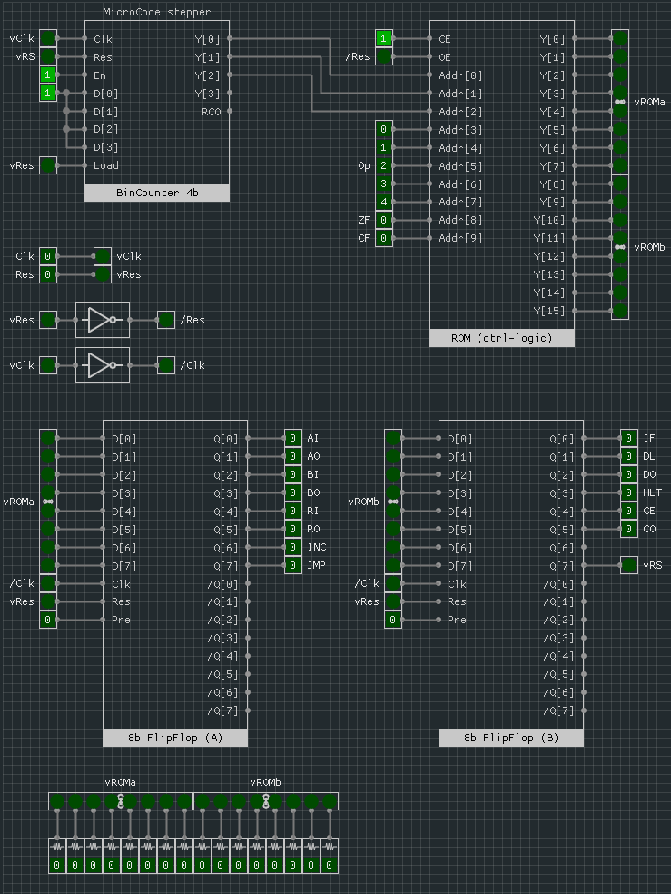
The Control module is in charge of outputting the signals that control the operation of the other modules. The computer uses 14 signals, of which the last one is internal to the control module:
| Index | Signal | Comment |
|---|---|---|
| 0 | AI | Load A-Register from data-bus |
| 1 | AO | Output A-Register to data-bus |
| 2 | BI | Load B-Register from data-bus |
| 3 | BO | Output B-Register to data-bus |
| 4 | RI | Write data-bus to current RA-address |
| 5 | RO | Output data at current RAM-address to data-bus |
| 6 | INC | Increment Program Counter |
| 7 | JMP | Jump to address currently on data-bus |
| 8 | IF | Instruction Decoder: load byte as opcode |
| 9 | DL | Instruction Decoder: load byte as data (output to data-bus) |
| 10 | DO | I/O-module: display data currently on data-bus |
| 11 | HLT | Halt the computer |
| 12 | CE | ALU: execute computation with current register-data |
| 13 | CO | ALU: output last computation to data-bus |
| 14 | - | not used |
| 15 | RS | Control Module: reset stepper to zero |
It uses a 16-bit ROM to map instructions to a sequence of output signal combinations. An instruction can consist of up to 8 sub-steps. Each word in the ROM contains state of the output signals per step. The ROM is addressed as follows:
| Addr[0:3] | Addr[3:7] | Addr[8:8] | Addr[9:9] |
|---|---|---|---|
| Step Index | Opcode-Instruction | ZF | CF |
By including the zero- and carry-flags in the address it’s possible to change the behavior of the instruction depending on those flags (i.e. jump when zero). It also means each instruction is repeated 4 times in the ROM.
As an example, the signal sequence for the LDA-instruction is:
| Step | AI | AO | BI | BO | RI | RO | INC | JMP | IF | DL | DO | HLT | CE | CO | - | RS |
|---|---|---|---|---|---|---|---|---|---|---|---|---|---|---|---|---|
| 0 | 0 | 0 | 0 | 0 | 0 | 0 | 0 | 0 | 1 | 0 | 0 | 0 | 0 | 0 | 0 | 0 |
| 1 | 0 | 0 | 0 | 0 | 0 | 0 | 1 | 0 | 0 | 0 | 0 | 0 | 0 | 0 | 0 | 0 |
| 2 | 1 | 0 | 0 | 0 | 0 | 1 | 0 | 0 | 0 | 0 | 0 | 0 | 0 | 0 | 0 | 0 |
| 3 | 0 | 0 | 0 | 0 | 0 | 0 | 0 | 0 | 0 | 0 | 0 | 0 | 0 | 0 | 0 | 1 |
The Random Access Memory
The last module of the computer is an 8-byte large static RAM-module. Like the ROM-modules, it is entirely built using basic LSim components. It’s a grid of 8-bit memory cells (built from D-latches). The address is fed through a demuxer to enable the required memory cell.
Besides the data-bus, there are 3 input signals: CE(Chip Enable), WE(Write Enable), OE(Output Enable). The RAM-module isn’t synchronized to the clock-module. The data-bus must be stable when WEis enabled.
Demo
Below you’ll find a link to a YouTube-video showing the 8-bit computer running a program that loops through the Fibonacci-sequence. The part that fits into an 8-bit register, that is :-)
Next steps
A project like this is never really finished; you can always find something else to add. Hi there, feature creep :-) But seriously, there are still some things that deserve to be worked on.
- I started with 4 seven-segment displays to allow the display to be switched between unsigned and signed-mode. Displaying the sign of the number as the first ‘digit’. I haven’t gotten around to implementing this. It would require changing the decoder ROM and either adding a switch to the I/O-module or a new opcode that displays a number in signed mode.
- Not all operations supported by the ALU have been surfaced in an opcode. Adding opcodes for the bitwise AND/OR/XOR operations is not that much work. I just haven’t found a good use-case for those instructions yet.
- The ‘L’ (for Logic) in ALU isn’t really implemented. You can test for equality by subtracting two numbers and checking the zero-flag. But it would be nice to be able to check if register-A is bigger than register-B. Maybe be abusing the carry-flag like in a 6502.
The biggest obstacle to adding more functionality is the limited output capability. There are only so many interesting things you can do when you’re limited to displaying an 8-bit integer. But adding more complicated displays, would stretch the scope of LSim beyond the feasible, I fear.
One other cool thing to do would be to build this computer with real hardware. Maybe using 74LS-logic chips and a few EEPROMS. It seems like an interesting way to take the first steps with KiCad and circuit board design.